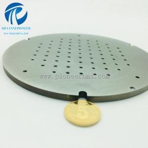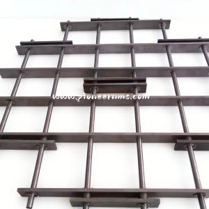
Semiconductor Grade High Purity Mo Target | PVD Sputtering for Solar & Display
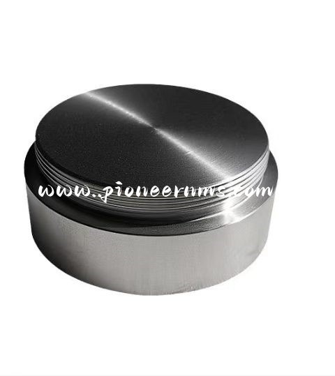
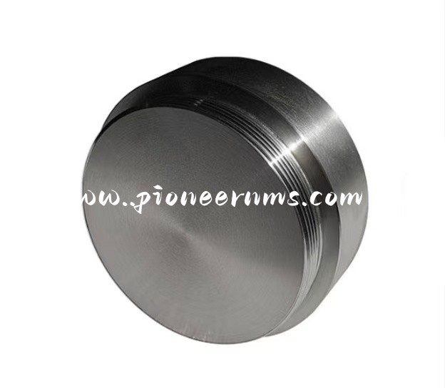
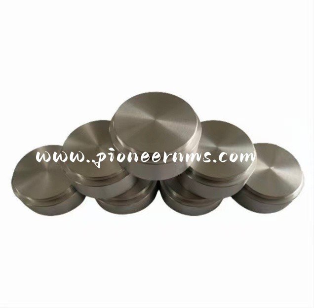
Our semiconductor-grade high purity molybdenum (Mo) sputtering target is specifically engineered for advanced PVD (physical vapor deposition) processes serving the solar photovoltaic and flat panel display industries. As an essential consumable in magnetron sputtering systems, this Mo target delivers superior thin film uniformity, high deposition rates, and ultra-low particle generation — critical performance attributes for high-volume manufacturing of solar cells and display panels.
Manufactured from premium molybdenum powder with purity levels reaching ≥99.95% (3N5) and optionally up to 99.99% (4N), our molybdenum sputtering targets meet the stringent cleanliness and performance standards demanded by semiconductor-grade production environments. The material undergoes advanced powder metallurgy and thermo-mechanical processing — including hot isostatic pressing (HIP), multi-directional forging, and precision annealing — to achieve a dense, fine-grained microstructure that ensures stable, reproducible sputtering performance throughout the target's full lifecycle.
Key Properties of Molybdenum for Solar & Display Applications
Molybdenum offers a unique combination of physical and electrical properties that make it the material of choice for both solar and display thin-film applications:
| Property | Value | Application Benefit |
|---|---|---|
| Melting Point | 2,617°C | Withstands high-power sputtering without deformation or warping |
| Electrical Resistivity | ≤7.5 μΩ·cm | Enables low-resistance electrodes and interconnect layers |
| Thermal Conductivity | 138 W/m·K | Efficient heat dissipation during prolonged sputtering runs |
| Thermal Expansion Coefficient | 4.8 × 10⁻⁶/K | Matches substrate expansion, minimizing thin-film stress |
| Density | ≥10.20 g/cm³ | Near-theoretical density ensures minimal porosity and stable sputtering |
| Crystal Structure | Body-Centered Cubic (BCC) | Provides excellent adhesion to glass, silicon, and compound semiconductor substrates |
Product Specifications
| Parameter | Specification |
|---|---|
| Material | Molybdenum (Mo) |
| Purity | ≥99.95% (3N5) standard; ≥99.97% (3N7) / ≥99.99% (4N) available upon request |
| Density | ≥10.20 g/cm³ (≥99.8% of theoretical density 10.22 g/cm³) |
| Average Grain Size | ≤100 μm standard; ≤80 μm / ≤50 μm optional |
| Crystal Orientation | Random or preferential (100)/(111) orientation available |
| Melting Point | 2,617°C |
| Thermal Conductivity | 138 – 139 W/m·K |
| Coefficient of Thermal Expansion | 4.8 – 5.1 × 10⁻⁶/K (at 25°C) |
| Electrical Resistivity (Target) | ≤7.5 μΩ·cm |
| Surface Roughness | Ra < 0.8 μm, Rmax < 10 μm |
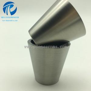
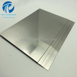
| Target Types | Planar (disc, rectangular, square) / Rotatable (cylindrical) |
| Bonding Options | Indium bonding or elastomer bonding to copper (Cu) backing plate |
| Planar Dimensions | Thickness: 3 – 32 mm; Diameter: up to 500 mm; Length: up to 1,500 mm; Width: up to 550 mm |
| Rotatable Dimensions | Length: up to 4,000 mm; Wall thickness: 5 – 20 mm; Outer diameter: 100 – 170 mm |
| Flatness | ≤0.2 mm (for planar targets) |
| Edge Finish | Chamfered / radiused edges per customer specification |
Applications
Solar Photovoltaics
-
CIGS / CIS Thin-Film Solar Cells: Molybdenum serves as the back-contact electrode layer, providing excellent ohmic contact, low sheet resistance, and effective barrier properties against selenium diffusion
-
a-Si / μc-Si Tandem Solar Cells: Functions as intermediate reflector layers and back electrodes in silicon-based thin-film photovoltaics
-
CdTe Solar Cells: Used as a stable metallic contact layer with good adhesion to CdTe absorber layers
-
Perovskite Solar Cells: Emerging applications as electrode and interfacial layers
Flat Panel Displays
-
TFT-LCD: Molybdenum and molybdenum-based alloy targets are used for gate electrodes, source/drain electrodes, and bus-bar lines in large-area display backplanes (generation 8.5, 8.6, 10.5)
-
OLED Displays: Serves as electrode layers and interconnection metals in both rigid and flexible OLED panel structures
-
Touch Panels: Used in metal mesh electrodes for large-size touch sensors and interactive displays
-
Micro-LED: Emerging high-resolution display applications requiring fine-pitch metal interconnects
Key Features & Advantages
1. Ultra-High Purity for Superior Film Quality
2. Optimized Microstructure for Consistent Sputtering
3. High Density for Extended Target Life
Achieving near-theoretical density (≥10.20 g/cm³) through our optimized manufacturing process significantly reduces internal porosity. This results in:
-
Reduced outgassing during vacuum sputtering
-
Minimized arcing and micro-arcing events
-
Improved film quality with fewer pinhole defects
-
Extended target utilization rates, particularly critical for expensive large-area targets
4. Advanced Thermal Management
Molybdenum's high thermal conductivity (≈138 W/m·K) combined with its low coefficient of thermal expansion ensures stable temperature distribution even during high-power-density sputtering. This prevents thermal stress-induced deformation, target cracking, and delamination from backing plates. For applications requiring enhanced cooling, our copper backing plate bonding service — available in both indium and elastomer formulations — further optimizes heat dissipation.
5. Versatile Configuration Options
-
Planar Targets: Available in disc, rectangular, and square configurations, suitable for laboratory R&D and production-scale sputtering systems
-
Rotatable Targets: Cylindrical design offering material utilization rates exceeding 80% (compared to ≤40% for planar targets), significantly reducing cost of ownership for high-volume manufacturing
-
Bonding Options: Indium bonding for high-power applications; elastomer bonding for thermal shock resistance and ease of target replacement
Customization Capabilities
We offer comprehensive customization services to meet specific process requirements:
| Customization Parameter | Available Options |
|---|---|
| Target Shape | Disc, rectangular, square, ring, stepped, or custom profile |
| Target Dimensions | Any size up to 1,500 mm (L) × 550 mm (W) for planar; up to 4,000 mm (L) for rotatable |
| Purity Grade | 99.95% (3N5) / 99.97% (3N7) / 99.99% (4N) |
| Grain Size | ≤100 μm / ≤80 μm / ≤50 μm |
| Hole Drilling | Standard hole patterns or custom mounting hole configurations |
| Edge Geometry | Custom chamfer angles, radii, and edge profiles |
| Backing Plate Material | Copper C10100 / C10200 with custom cooling channel designs |
| Surface Finish | As-sputtered, ground, polished, or custom surface roughness |
| Marking | Laser-engraved part numbers, logos, or batch identifiers |
| Packaging | Standard or cleanroom Class 100 packaging with vacuum sealing |
Each shipment includes a comprehensive Material Test Report (MTR) with full traceability from raw powder to finished target, providing complete documentation for quality audits and process validation.
Why Choose Us
-
Semiconductor-Grade Quality: Our manufacturing processes are aligned with the quality standards of the semiconductor and display industries
-
Consistent Purity: Rigorous raw material selection and in-process quality control ensure batch-to-batch consistency
-
Technical Support: Our engineering team provides application support, process optimization, and troubleshooting assistance
-
Flexible Manufacturing: From R&D-scale small batches to high-volume production quantities
-
Global Delivery: Efficient logistics network ensuring on-time delivery worldwide
-
Competitive Pricing: Direct manufacturing with optimized production processes delivers exceptional value
For technical specifications, customized solutions, or to request a quotation, please contact our sales team with your detailed requirements.